Random-access memory: Difference between revisions
RAM stub |
RAM construction |
||
| (2 intermediate revisions by the same user not shown) | |||
| Line 2: | Line 2: | ||
{{RAM}} | {{RAM}} | ||
RAM is composed of multiple cells that store data | '''RAM''' is composed of multiple cells that store data, accessed by an address.<br> | ||
It has 4 inputs: | It has 4 inputs: | ||
#Data input | # Data input | ||
#Address input | # Address input | ||
#Write signal | # Write signal | ||
#Read signal | # Read signal | ||
And 1 output: | And 1 output: | ||
#Data output | # Data output | ||
Each cell in RAM is essentially a [[register]]. | |||
Building a RAM from scratch is one of the best ways to start learning logic and computers, as well as to get familiar with circuit construction in ''Logic World''. | |||
RAMs can have very different designs, specifications, and can be [[Optimization|optimized]] for speed, size, or even aesthetics. RAM designs are usually specified by the following parameters: | |||
# Address size | |||
# Data size | |||
# Delay during retrieving/storing data | |||
# Speed between sequential operations | |||
''' | '''Address and data size''' is determined by the number of bits. The total number of combinations using '''n''' bits is <math>2^n</math>. | ||
''' | '''Delay''' during retrieving/storing data is the time between when the read/write signal is turned {{on}} and when the data is retrieved or stored for a single operation. | ||
This article will | '''Speed between sequential operations''' is how fast the RAM can run multiple sequential operations. The delay between multiple operations is always <math>\ge</math> the delay for a single operation. | ||
This article will demonstrate a simple RAM with 4 bits for address and 8 bits for data. | |||
== Construction == | == Construction == | ||
Before constructing a RAM circuit, you need to decide how many memory cells are required and how wide each cell should be. | |||
In the following example, there are 16 memory cells, each 8 bits wide. | |||
Using the formula <math>b = \log_2(x)</math>, you can see that to address 16 different memory cells, 4 bits are needed. | |||
It is possible to use a single [[decoder]] to select the address, but in this example two decoders are used to specify the row and the column of the memory matrix. This makes the structure easier to understand, and also results in decoders that are half the size. | |||
[[File:2-decoders-ram.png|thumb|right|alt=Two 2-bit decoders placed orthogonal|Two 2-bit decoders placed orthogonal]] | |||
On the screenshot, you can see the two decoders placed orthogonally. Above them is the 4-bit address input. | |||
<div style="clear:right;"></div> | |||
[[File:Ram-register.png|thumb|right|alt=A register for a cell|A register for a cell]] | |||
For each cell, we use a simple 8-bit [[register]], shown in the next screenshot. | |||
It has one [[AND_Gate|AND]] gate to combine the row and column signals. This enables the register if it is at the selected intersection. | |||
It also has a separate signal for writing data and another for reading. | |||
<div style="clear:right;"></div> | |||
[[File:Ram-stage-2.png|thumb|right|alt=16 cells placed in a grid|16 cells placed in a grid]] | |||
This register is copied 16 times and arranged into a 4×4 grid. The result is shown on the next screenshot. | |||
<div style="clear:right;"></div> | |||
[[File:Ram-stage-3.png|thumb|right|alt=Address and signal wires connected|Address and signal wires connected]] | |||
The next step is connecting wires from the decoders to the cells, row by row and column by column. | |||
Wires are routed in 3D on top of the cells. | |||
Write and Read signals are also added. The new wiring is highlighted in yellow. The top-left cell (address 0) is selected, but it will not perform any operation unless a Write or Read signal is activated. | |||
<div style="clear:right;"></div> | |||
The last step is connecting the data inputs and outputs. | |||
The input is placed on the top, and all bits are connected to the corresponding inputs of every cell. | |||
The same is done for the output, which is placed on the bottom. | |||
Note that the input and output bits are shared. This is not a problem as long as reading and writing are not performed at the same time. | |||
The final screenshot shows the completed RAM circuit. It has 2 cells with stored data, and it is currently reading from the cell at address 6. | |||
[[File:Ram-final.png|frame|center|alt=Completed RAM circuit, reading data|Completed RAM circuit, reading data]] | |||
== See also == | == See also == | ||
* [[Mods:CheeseUtilMod|CheeseUtilMod]] - a mod with RAM components | * [[Mods:CheeseUtilMod|CheeseUtilMod]] - a mod with RAM components | ||
Latest revision as of 15:41, 14 September 2025
- Random-access memory
- In Logic World, Random-access memory (RAM) is a circuit that can store and load data on demand.
- Unlike ROM, the contents of RAM can be changed at any time by writing new data to it.
- Unlike non-random-access memory, access can be performed in any order with a constant delay for each cell.
RAM is composed of multiple cells that store data, accessed by an address.
It has 4 inputs:
- Data input
- Address input
- Write signal
- Read signal
And 1 output:
- Data output
Each cell in RAM is essentially a register.
Building a RAM from scratch is one of the best ways to start learning logic and computers, as well as to get familiar with circuit construction in Logic World.
RAMs can have very different designs, specifications, and can be optimized for speed, size, or even aesthetics. RAM designs are usually specified by the following parameters:
- Address size
- Data size
- Delay during retrieving/storing data
- Speed between sequential operations
Address and data size is determined by the number of bits. The total number of combinations using n bits is .
Delay during retrieving/storing data is the time between when the read/write signal is turned ON and when the data is retrieved or stored for a single operation.
Speed between sequential operations is how fast the RAM can run multiple sequential operations. The delay between multiple operations is always the delay for a single operation.
This article will demonstrate a simple RAM with 4 bits for address and 8 bits for data.
Construction
Before constructing a RAM circuit, you need to decide how many memory cells are required and how wide each cell should be. In the following example, there are 16 memory cells, each 8 bits wide.
Using the formula , you can see that to address 16 different memory cells, 4 bits are needed. It is possible to use a single decoder to select the address, but in this example two decoders are used to specify the row and the column of the memory matrix. This makes the structure easier to understand, and also results in decoders that are half the size.
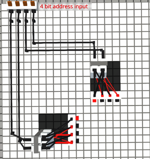
On the screenshot, you can see the two decoders placed orthogonally. Above them is the 4-bit address input.
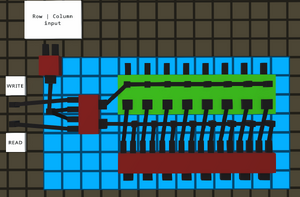
For each cell, we use a simple 8-bit register, shown in the next screenshot. It has one AND gate to combine the row and column signals. This enables the register if it is at the selected intersection. It also has a separate signal for writing data and another for reading.
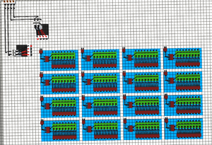
This register is copied 16 times and arranged into a 4×4 grid. The result is shown on the next screenshot.
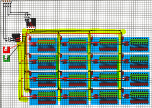
The next step is connecting wires from the decoders to the cells, row by row and column by column. Wires are routed in 3D on top of the cells. Write and Read signals are also added. The new wiring is highlighted in yellow. The top-left cell (address 0) is selected, but it will not perform any operation unless a Write or Read signal is activated.
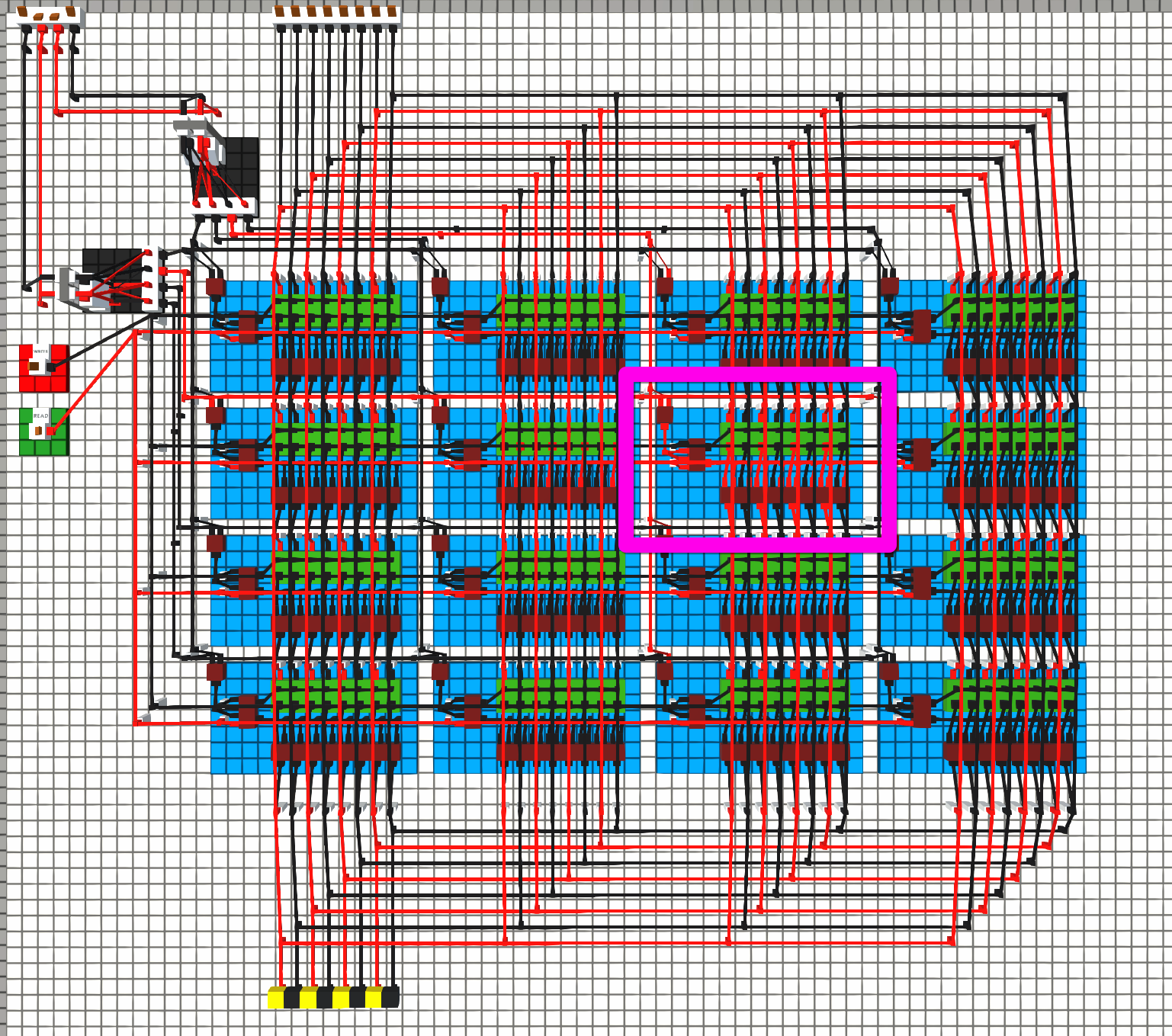
The last step is connecting the data inputs and outputs. The input is placed on the top, and all bits are connected to the corresponding inputs of every cell. The same is done for the output, which is placed on the bottom.
Note that the input and output bits are shared. This is not a problem as long as reading and writing are not performed at the same time.
The final screenshot shows the completed RAM circuit. It has 2 cells with stored data, and it is currently reading from the cell at address 6.
See also
- CheeseUtilMod - a mod with RAM components

